中学のときに第1号機を作りました。高校生のときにはマイクのスイッチで
リレーを動かして送受信切り替えを行う2号機を作りましたが、2号機は
実際の交信に使うことはありませんでした。でも、また作りたくなって作り
ました。歳を取って少年時代の思い出に浸って。
しかし、昔と同じ物を作ったのではつまらないので、光波無線の製品のよ
うにプラグインコイル式にしようかと思ったのですが、小型のケースに入れ
るとプラグインコイルは不向きですので、やめました。結局、電源以外は
科学教材社バージョンの回路で、B電源は倍電圧整流し、IC と Power MOS
FET で安定化して送信周波数を安定化したつもりです。また、小型化する
ためにトランスレスにし、ヒーターはフィルムコンデンサを直列に入れて
電圧を下げました。
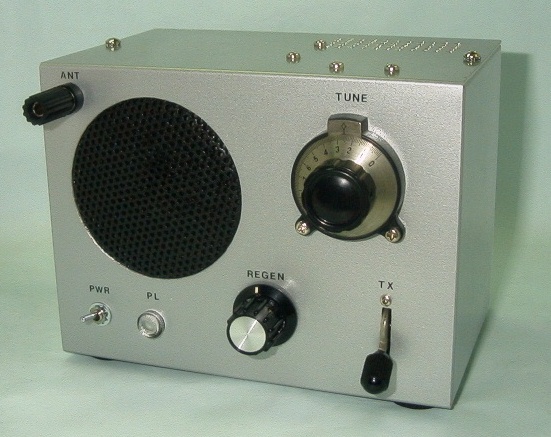
ケースはタカチの MB-22 という 120x100x160mm のサイズで、片手に乗る
かわいいものです。その形とスピーカーグリルの様子は、昔の江角電波の
超再生式トランシーバから少し影響を受けています。
配線さえ合っていれば簡単に動作するだろうと思っていたら、トラブル続
出でした。
①B電圧の安定化回路が発振した。
LM317T の出力側に 0.1uF を入れたら止まりました。この回路は何度も作ったのですが、発振はしなかったのに。
②B電圧の安定度が悪かった。
出力電圧が低目のときに、入力電圧を変動させると、出力電圧がかなり変動してしまいました。これは Power MOS FET のバイアス電圧を作る 9V の定電圧ダイオードの電流を 5mA から 2mA 程度に減らしたら直りました。
③低周波増幅回路が発振した。負帰還はかけてないのに!
最初、昔の科学教材社の製品の回路通りにグリッドリークバイアス式の電圧増幅回路にしたところ、入力インピーダンスが非常に高くなり、シーメンスキーの送信側接点(低周波増幅段の出力トランスの一次側につながっている)から受信側接点(低周波増幅段の入力がつながっている)へ信号が帰還された(絶縁がそれほど高くなかった)ためだと、回路図と現物を眺めていて思いました。目視では絶縁が悪いようには見えませんでしたが。
そこで、電圧増幅段を自己バイアスにし、グリッドリークを 220kΩにしたら止まりました。
④ハムが多かった。
トランスレスであることと超再生検波方式のためか、ハムが盛大に出ました。AC100V 端子間に 0.01uF を入れたり、ヒーターのパスコンをつなぐ位置を変えたりして、超再生のノイズに隠れて気にならないレベルにまで減りました。なぜか、シャーシとB電源間のパスコンもハムの量に影響がありました。
今回はスペアナで大体の送受信周波数を合わせ、オシロで低周波増幅段の波形を見てトラブルシューティングをしました。中学時代に初めて作ったときには、よくトラブルなしに動いたものです。当時のはトランスレスではなかったし、電源は普通のトランス式だったからでしょうね。
本機の場合には正常なのですが、子供の頃感じた変調の浅さが、オシロでRFの波形を見て確認できました。一応、変調器となる部分のゲインを多めにしたのですが。
また、ボディーエフェクトたのめ、送信周波数が 50kHz くらい変動するので、相手も学研の「ラジホーン」みたいな超再生式のトランシーバでないと、まともに交信できません。バリコンとダイヤルのあいだにはカプラーが入れて絶縁してあるんですが。
I built a two-tube transceiver for the 27MHz CB band with a super
regenerative circuit when I was 13 and another one when I was 16.
The second one uses a relay as the transmit-receive switch.
So, this is my 3rd one. This time, I chose a small enclosure (120x
100x160mm) . To pack the components into the small enclosure, I
did not use a power transformer and used the doubler rectifier
circuit and a regulator circuit using the LM317T and a power MOS
FET hoping that the transmitting frequency will be stable.
Contrary to my expectation, I had many troubles as below.
(1) The regulator circuit oscillated.
Adding a 0.1uF capacitor to the output of the LM317T fixed this problem.
(2) The regulation of the regulator circuit was bad.
This was due to inaprroptiate current of a zener diode that
makes a bias voltage for the power MOS FET.
(3) Audio amplifier oscillated without negative feedback.
The original audio voltage amplifier circuit used the grid leak bias. I thought this made the input impedance very hight and the feedback occurred through the Siemens key switch (transmit-receive switch).
So, I changed the bias to the self bias and used 220k ohm sa
the grid leak. These changes fixed the problem.
(4) Large hum noise.
This may be because of the transformer-less power supply.
Adding a 0.01uF capacitor accross the AC 100V and changing the bypass capacitor for the heater circuit reduced the hum noise.
This time, different from dacades ago, I was able to use a spectrum analyzer to adjust the frequency and an oscilloscope to fix the oscillation problems. This made me think how good the original design was because I was able to build the first one without problems.
One problem with the design is that the modulation index is low
(A-B/A+B is small). Another problem is that the transmitting
frequency is not stable due to the body effect. So, communicating with a transceiver with super-regenerative receiver is fine but with a superhet receiver is not practical.